Markets & Applications
Introduction
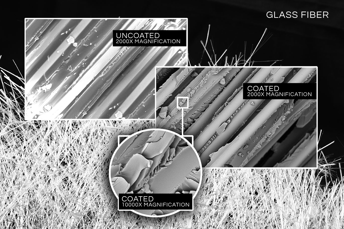
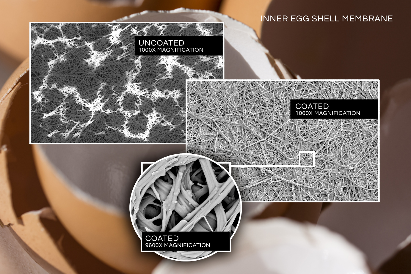
Electron microscopy (SEM and TEM) techniques offer researchers worldwide the ability to generate images with amazing detail and high resolution. However, the use of an electron beam in these techniques may present problems with materials that are poorly electrically conductive or heat sensitive.
Certain settings in the SEM can reduce these effects (read more), but the preferred solution is to treat such samples with a continuous, conductive thin film via sputter coating .
For TEM, the classic application is coating grids with carbon. This also provides additional support for fragile or non embedded samples. Moreover, carbon is a good conductor, performing a similar role as the metal coating in SEM applications.


Applications
For researchers and scientists seeking to understand more about the structure, performance and properties of materials, electron microscopy is an essential tool. In addition, thousands of labs worldwide use this technology every day for quality control of consumer products, diagnoses of disease and safety issues, and also for example, for forensic decision-making.
Scientists and engineers must be able to rely on consistent and reliable results for all of these applications. For electron microscopy, this means that a metal sputter coating step will often precede imaging.
Markets
Material sciences
Material sciences comprises many different branches and covers a wide range of materials like polymers, filters, metals, pharma, textiles, coatings, ceramics, life science applications, electronics, and so on.
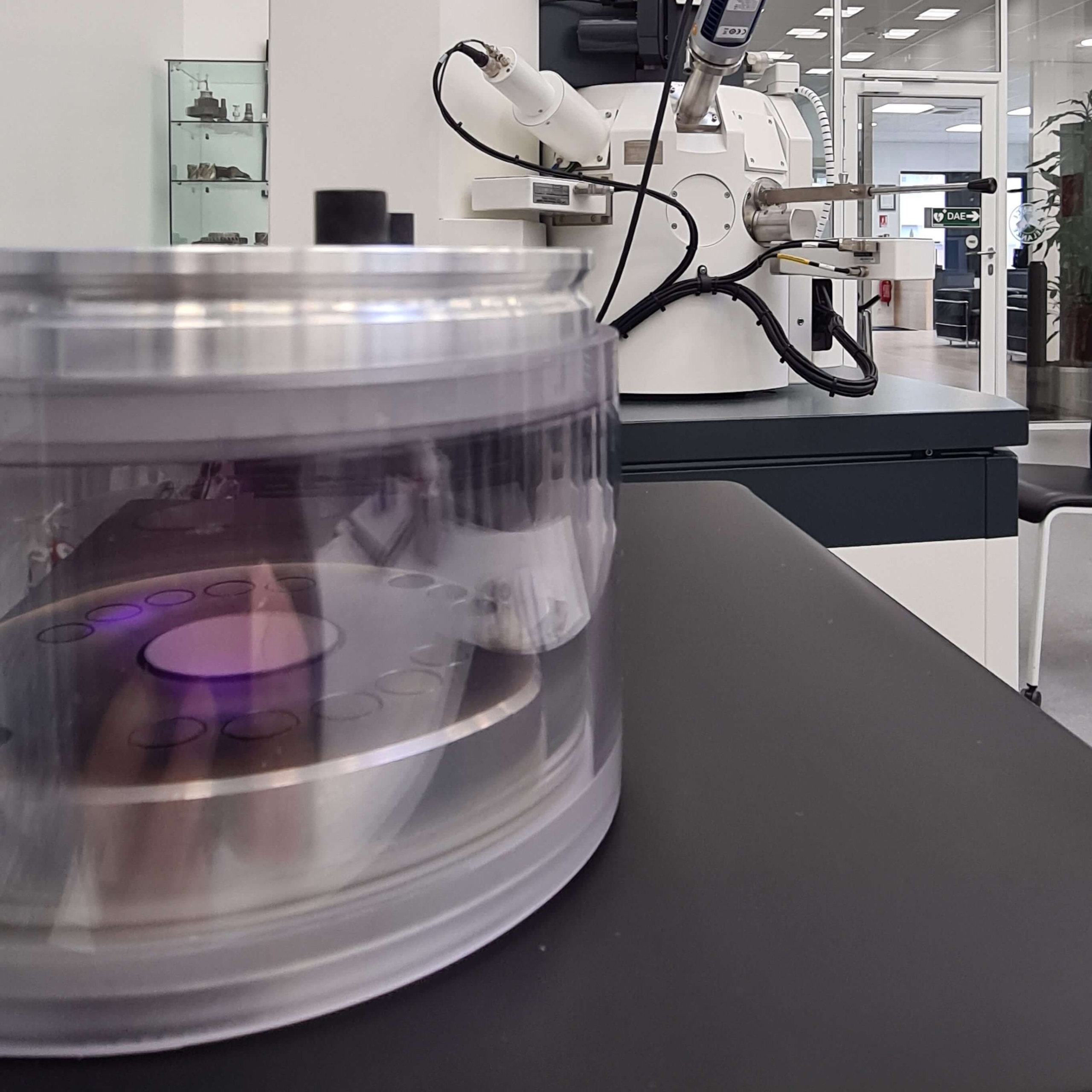
The LUXORAu and LUXORPt metal coaters are widely used for all of these applications, particularly for electron microscopy (SEM and FEG-SEM) purposes where sample charging might be an issue, and when working with beam sensitive materials.
The list of material sciences applications ranges from particle characterization, analysis of the micromechanics, visualizing the morphology of plastics, root cause analysis and chemical composition and homogeneity of materials, etc…
Todays’ materials science labs have become a central hub for product development, solving customer issues and high level quality control applications. Despite a wide diversity of incoming materials and their related issues, reproducible and user friendly testing methods have to be readily available and accessible to operators who only have a limited knowledge of the equipment. Moreover speedy and high throughput solutions are crucial to cope with the everyday work.
This is why the LUXOR fully automated metal sputter coater fits perfectly in your lab.
In the LUXOR knowledge center you will find application notes and technical guides that are of interest for a wide range of industrial and academic environments.

Academic applications
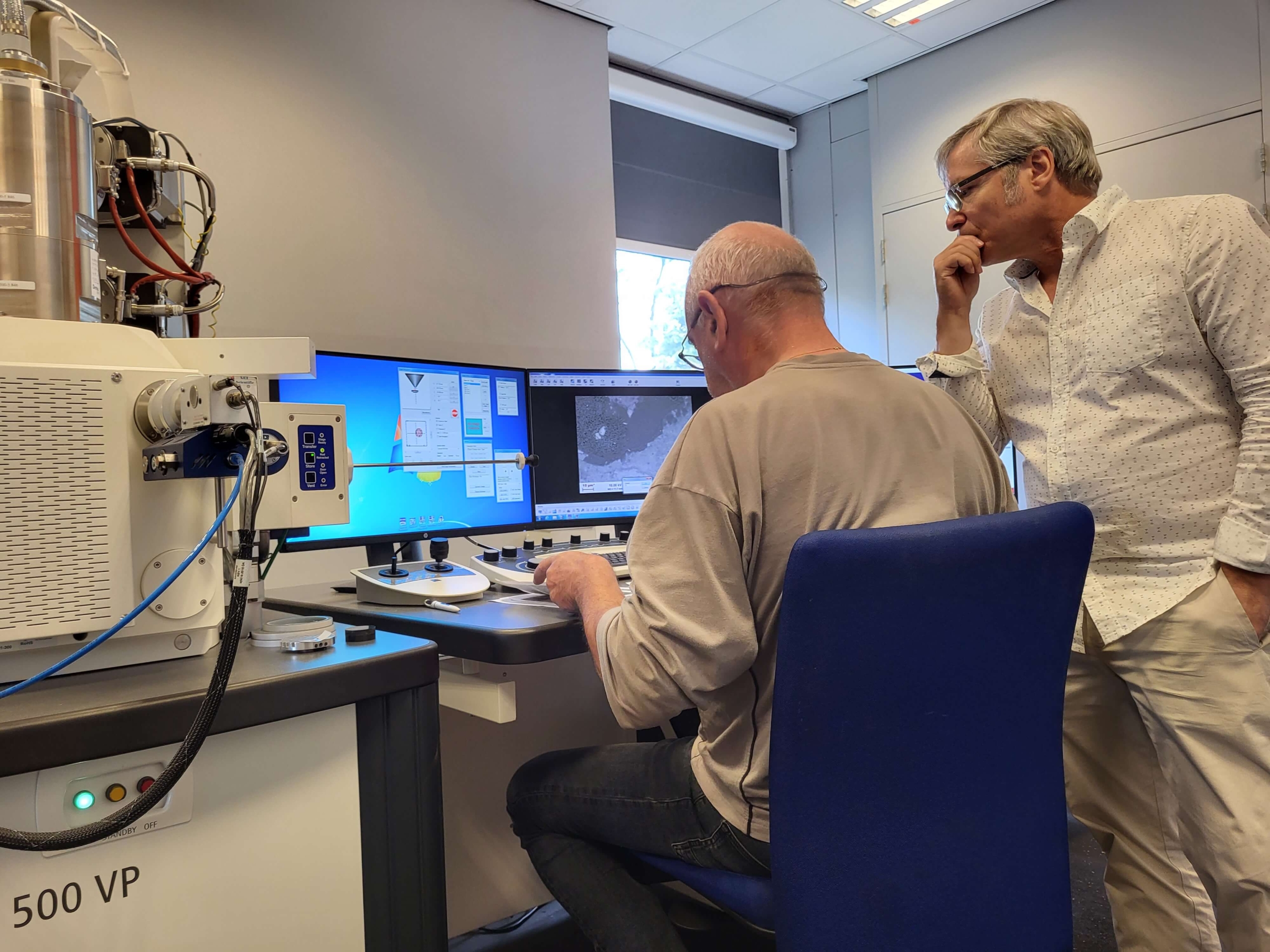
Working properly with a SEM or FEG-SEM microscope demands – amongst other things – for extensive knowledge about sample preparation.
To this end, the leading scientists of tomorrow learn how to work with LUXOR coaters in universities all over the world.
The LUXORAu and LUXORPt metal coaters can handle a wide diversity of sample materials, shapes and forms, and are therefore particularly suitable for academic applications. Visit our accessories page and learn more about our range of sample holders and target materials.
In a university setting, many different operators, ranging from students to senior researchers are using SEM technology and related sample preparation techniques such as sputter coating on a daily basis. There is also the wide diversity of specimens and materials for which a reliable sample preparation technique is essential.
Thanks to the fully automated operation and the optimised user interface of the LUXOR coater, the chance of human errors is minimal.
In the LUXOR knowledge center you will find application notes and technical guides that are of interest for a wide range of industrial and academic environments


